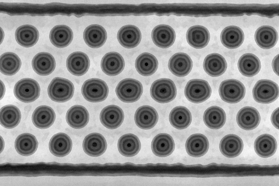
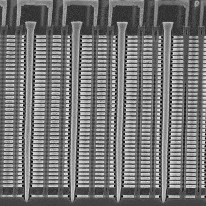
3D NAND Metrology Workflow
Automated navigation, imaging and metrology of 3D NAND memory structures in a scanning electron microscope.
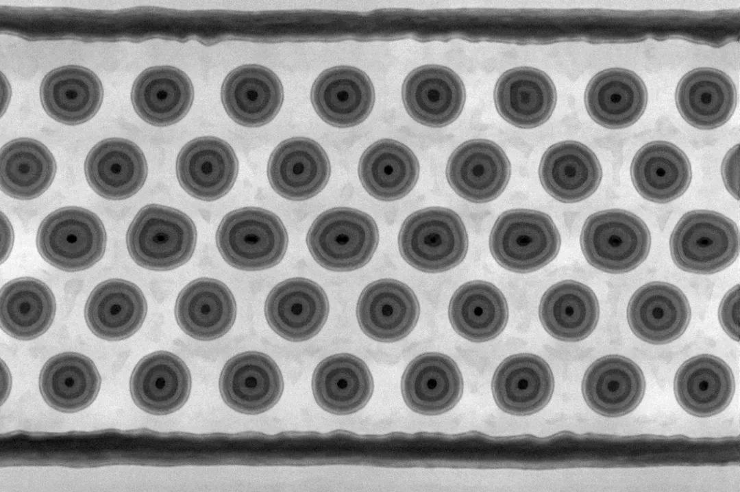
3D NAND memory stacks hundreds of layers of memory cells on top of each other, with vertical channels running through the whole stack. Inspecting it in an electron microscope means finding and imaging the right spots in a large, highly repetitive structure where almost everything looks the same. Done by hand, it is slow and hard to reproduce.
I worked on automating this workflow: software that navigates the sample on its own, decides how each region is imaged and keeps the beam aligned during long unattended runs.
The other half was metrology. Processing the acquired images offline and measuring the structures gave us an objective way to tell whether a change to the workflow actually improved the results, instead of judging by how the images looked.
Gallery